(1 week)
In this lab, you will create a scrolling message display using the two 7-segment LEDs on the XSTends board. The message will be loaded into RAM at address 0 using GXSLOAD at the same time that you load your .bit file. The message will consist of the ASCII code for each letter in the message. You will be provided with a partial design that you will need to complete.
The clock source for this lab will come from the 16 KHz pin of a OSC4 component. A control unit will divide the frequency of this clock so that each character is displayed long enough to be read by a human. You may think that we should simply use a slower clock speed (for example, the OSC4 has a 15 Hz pin, which would not need to be slowed down so much). But there is a glitch: the LEDs on the XStends board use the same lines that are used to address the RAM. The sharing of wiring resources (and chip pins) on a board is a common occurrence in digital designs. If you check the XStends manual, you will see that nearly all the FPGA pins are connected to two or three components, not just the one that you would probably expect. Perhaps the most well known examples of this sharing are the main busses used in modern computer systems - the PCI bus and the older ISA bus. The same situation exists between the computers on the same network.
Since this sharing is so common, there are obviously some standard techniques to implement it. These "sharing methods" are usually refereed to as multiplexing. Multiplexing refers to dividing some shared resource into parts, with each part given to each "interested party". One common example of multiplexing is Frequency Division Multiplexing (FDM), which divides the available frequencies on the carrier (i.e. the wire, optical cable, air waves) into discrete intervals, with each component receiving one interval for their exclusive use. Multiplexing is what allows multiple radio stations to broadcast in the same airspace, multiple cable TV stations to broadcast on a single cable line, or 20 simultaneous telephone conversations to pass through the same single copper wire. Another common multiplexing technique is Time Division Multiplexing (TDM). IN TDM each component gets the entire channel, but only for a small portion of the time. This is commonly used within computer systems. For example, when several programs try to access large files on a hard drive, they each get a portion of its file every so often (rather than serving the first program it's entire file, then the next, and so on...).
In order to solve the problem of the RAM and LEDs sharing the same bus, we will use Time Division Multiplexing. Of course, when we access the RAM, the RAM addresses will also appear on the LEDs because there is no way to tell the LEDs about our multiplexing scheme so that the LEDs "stop listening" for a while (we have this capability on the RAM, since it has an enable(/disable) line). Fortunately LEDs have a slow response time: if the signal is toggled quickly enough, the LED does not have time to react to the change. Thus, we will exploit this property to make the RAM accesses invisible to an observer by using only a couple of clock cycles (at 16 KHz) to access the RAM, and then a large number (about 8000, which is about 1/2 second in this frequency) to output to the LEDs. At this rate, only an astute observer in a dark room could detect the faint flicker produced by the RAM accesses. If the flickering were to become a problem, the design could be modified very easily to use the 50 MHz oscillator on the XS40 board to make these flickers imperceptible. We would just need a bigger counter.
With each repetition of this 8000-step cycle, the following steps will
occur:
0. Read the lab assignment. Read the GXSLOAD sections related to using RAM. Read pages 854 - 858 (sections 10.2 - first half of 10.3.3) in Wakerly.
1. Using the methods and techniques learned in class (i.e. Karnaugh maps),
design a 4-bit binary counter (with reset input). You may use D, T, or JK
flip-flops (these are the only kinds available in the Foundation schematic
editor, where you will implement your design) and primitive logic gates
only. Also, sketch a schematic of the counter.
Note: It is very important to design your counter BEFORE coming to the
lab - you WILL NOT have time to do this and the rest of the lab during the
lab period!
2. Read the VHDL code for the control and linesel units (see the resources section below). Think about how you will complete them. You may want to start filling in the missing sections of code before coming to the lab. Note that these VHDL files should synthesize, but since there is no functional code in them, they won't do anything. You may also want to look at the schematic to see how the system is laid out. You can also save some time in the lab by reconstituting the project before coming to the lab. Instructions for this can be found in Space Management .
3. Reconstitute the provided project using the process outlined in Space Management .
4. Fill in the missing sections of the VHDL code (comments in the files will instruct you on what you need to do).
5. On a new schematic sheet, implement your 4-bit counter. Simulate the operation of the counter in the functional simulator and save the waveform for inclusion in your report. Then, create a macro from that sheet ( here's how ). Remember to include this schematic in your report.
6. Create another macro from a new sheet that implements a 16-bit counter (for the address counter) by chaining several of your 4-bit counters together. Use Hierarchy connectors for the clk and rst inputs, but for the output, use a bus. You will need to use bus taps to connect the individual lines from the 4-bit counters to the bus. In order to make the bus an output port, select the bus tool and draw the bus in an open area (where you will connect it to the counters, probably a long vertical bus). When you have a long enough bus, double click, and a dialog will open: "Add Bus Terminal/Label". Enter the name of the bus (this will be the name of the output pin), and make sure that it's range is [15:0], and that the terminal type is "output". When you click OK, the bus will be drawn, and there will be a terminal at the end of it. Now you can tap the bus. Make sure that you connect the right counter pins to the right lines of the bus! You may wish to simulate the 16-bit counter to make sure that you connected everything correctly (not required, but at least a partial simulation is recommended). Remember to include this schematic in your lab report.
7. Replace the 16-bit counter that is currently in the schematic (CB16CE) with the one 16-bit macro symbol you just created. You may want to keep the CB16CE in the design until you are sure that you have correctly completed the VHDL modules.
Notes about RAM:
Remember that in order to use the RAM, you need to assert the chip select (CEB) line to enable the RAM, and the output enable (OEB) line to get the RAM contents out on the data lines. For this lab, since we only read from the RAM, you can just assert CEB and OEB continually. However, the RAM lines are active-low, so you will want to tie CEB (p65) and OEB (p61) to GND to enable them, NOT VCC. Conversely, you may want to tie write enable (WEB, p62) to VCC to disable writing to the RAM. In a more complicated design (like lab 6) you will need to use control logic to keep these lines in the correct state (as you can see, CEB and OEB have already been connected to ground for you this time).
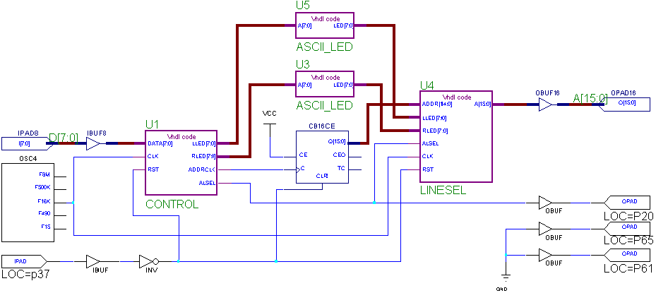
This is what the initial schematic should look like. If the wires are not connected correctly, be sure to fix them! Once you start working on the lab, you will probably want to spread things out a little to give yourself room to work (I had to squeeze things in so that the image was a reasonable size). This lab has been created using the name "lab4dsgn." If you want to use a different name, you need to rename the schematic and constraint files to the new name. Here are the files you need:
ASCII display unit VHDL code (or txt ) Note: ASCII input should be UPPERCASE letters. Also note that this unit is targeted at the active-high LEDs on the XS40 board. For use with the active-low LEDs on the XSTends board, you will need to invert the output (a INV8 should do nicely, or do this in the linesel unit).
Control Unit VHDL code (or txt ) Buffers LED contents, and controls the switching between RAM access and LED display. Note: you need to complete the code for this unit.
Line Selection Unit VHDL code (or txt ) Selects the right data to put on the output lines, depending on whether we are doing RAM access or LED display. Note: you need to complete the code for this unit.
User Constraint File lab4dsgn.ucf Pin Assignments for the I/O busses (address/led out and Data in)
Schematic Diagram lab4dsg1.sch Schematic for the partially completed project.
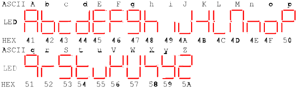
Here is a table of ASCII Codes , just in case you are interested (not required to do the lab)
Display characters: Some imagination may be required
for the K, M, V, W, and X, since it is rather difficult to make all 26 letters
display distinctly and recognizably in a single digit LED without diagonals.
However, this is typical for logic design, where creativity and compromise
are constantly required. Note that the ASCII line shows the what character
the LED is trying to resemble, but all the codes (input to the display
unit) on the HEX line are for the UPPERCASE letters, which is what the display
unit expects. Unknown codes (such as lower case letters) will result
in nothing being displayed.
Test Messages (Intel HEX files, to load into RAM):
[Return to CMPUT 329 Lab Home Page]