
Q: Once I've built a VHDL or FSM module, what is the best way
to edit it?
A: Use the Hierarchy Push/Pop tool . This will
open the editor for that module already loaded with the code/state machine.
Do your changes, update the macro and exit the editor - the changes will
automatically be applied to your schematic (you may get warnings it you
change pin assignments).
. This will
open the editor for that module already loaded with the code/state machine.
Do your changes, update the macro and exit the editor - the changes will
automatically be applied to your schematic (you may get warnings it you
change pin assignments).
Q: Something is wrong with my schematic and I can't seem to fix it or even find out what the problem is.
A: Be sure to check the implementation report files - look for warnings and errors - especially in the translate and map reports. Also, look for removed logic.
Q: How do I save an Image of my schematic so I can include it in my lab report later?
A: You need to do a screen capture. To do this, get the portion of the schematic that you want to caputre in the visible area of the editor. Zoom appropriately, and remember that the quality of the captured image is determined by the quality of what you see - so don't zoom out too far (What You See Is What You Get!). When you are ready, press ALT+Print Screen (Print screen is above Insert/Home/Page up). Now, go into Paint and paste the capture in. To open Paint: Start -> Programs -> Accessories -> Paint, then press CTRL+V or select Edit -> Paste from the menu. You will need to crop the image to remove the extra parts of the capture, such as the toolbars. You can crop the top and left by selecting the entire image and then moving the selection up and to the left. Crop the bottom and right sides by grabbing the handle at the bottom right of the drawing area (it is gray, and hard to see, but your cursor will change when your mouse is over it) and drag it in over the image. Save the .bmp file. If you don't like .bmp files, you can use a 'nix box and use tools like xv or gimp to convert it to a different format.
Q: What are IBUF, OBUF, BUFG, IPAD, OPAD, and IOPAD?
A: Read the descriptions of parts at the bottom of the component list when you click on them in the schematic editor:
Q: How do I Assign PADs to FPGA pins?
A: You have 2 options.
1. For single PADs only (not busses). Double click the PAD to get the Symbol Properties page. In the "Parameters" section, type "loc" as the name, and "Pxx" as the description (where Pxx is the pin, eg. p20 for pin 20 (middle segment of the LED)) . Then click add (to the right), and "LOC = P20" will appear in the list. Then click OK to exit this page. A label like "LOC = P20" will appear below the pad. You can move the label by click and drag. If you need to change the pin assignment, do the same thing, but instead of typing in the information, select it from the list, change the pin number (the description), and click change (instead of add).
2. For any PAD. First, you need to name the wire (net) that enters the PAD. Then, you need to edit the<proj_name>.ucf file in the project's directory. You probably want to add this to the files list in the Project Manage (main screen) - Select Add Source Files from the Project menu, then find the .ucf file. Now that the file is on the list, you can just double click it to edit it. The default file has lots of examples written in it, but everything is commented out (with #). You can delete all that, or just add what you need. Here's what you need to add:
NET <net_name> LOC = Pxx;
where net_name is the name you gave the wire, and Pxx is the pin number you are assigning the net (eg P20).
If the net is a bus, then you need to assign a pin to each (used) line of the bus. To do this, use the same statement as above, but replace net_name withbus_name<line>.
Eg: (This conencts a bus to the 7-segment LED on the
XS40)
NET CLK LOC = P13; -- assigns the net CLK (case sensitive) to pin 13
(clock input)
NET LED<0> LOC = P25; -- assign line 0 of bus LED to pin 25 (LED
segment 0)
NET LED<1> LOC = P26; -- assign the rest of the lines to the other
segments
NET LED<2> LOC = P24;
NET LED<3> LOC = P20;
NET LED<4> LOC = P23;
NET LED<5> LOC = P18;
NET LED<6> LOC = P19;
-- Even though this is probably an 8-line bus, though an OBUF8 and an OPAD8, line 7 is not connected (since there are only 7 segments). Foundation will remove all the lines and logic for line 7, since it is not used. However, there may be warnings about unmatched bus widths (since this is probably a 7-line output, but is running through an 8-line bus).
****NOTE: When you use the UCF file, remember: When you implement your
design, the current .ucf file is made part of the project. If you re-implement,
the old/first .ucf file will be used. Thus, if you change net names, you
will get errors. Also, changed pin assignments or new nets/pin assignments
will not take effect. To avoid this, you need to delete the previous
implemntation, from the Versions tab in the project manager.
Q: How do I name a wire (net) so I can use it in the UCF file or Simulator?
A: Double click the wire, and enter the name.
Q: How do I know which pins are what?
A: read the XS40 manual (PDF) - the 3rd last page lists all pins, the next 2 pages have schematic diagrams of the circuitry. If you are using components on the XSTends board, you may want to check the XSTends manual (PDF). You can also find more information on XS40 pins from EE183 at Stanford.
Q: How to connect components with wires?
A: if you want to move wires, click and drag them. NOTE: if there is a connection or branch, it will "hold" a part of the wire - it is better to move the connection, unless you don't want it to move.
Q: Can you rotate components?
A: Yes - right-click the component, select properties, click attributes button, select the rotation desired.
Q: Can I zoom in on part of my design easily?
A: hold ctrl+shift, and then L-click/drag a box around the area to zoom-fit
to.
Q: How come it makes crazy (looped, goes through the component...) wires, and how do I fix it?
A: It is trying to make a path that does not come too close to any components, and has as few as possible crossings with other wires. Sometimes it gets confused/gives up and you get bad results. FIX: move the connected components to unkink the wire. ie. move a component so that something like |_| becomes |___ . Repeat until wire is more or less straight. Then move components to desired location, and the path should be made properly. Alternatively, you can grab the wire and move it (click and drag it). However, this can be tricky.
Note that if you are moving the wire, it will bend to let you move a section if the ends are connected to fixed spots such as components or branches (you have to click exactly on the little dot to move the intersection point).
ALSO: If you move components around to make more space, then hit CTRL+W, it will re-route the wires to make it nicer. (or selectEdit->Redraw Wires).
HINT: placing components farther apart at first tends to produce fewer crazy wires (more space for path-finding).
Q: Why does a connected (I checked) wire has no load?
A: Make sure the destination uses the input. For example, the input is in the signal list of a process() statement (in VHDL) or is used in a state machine (eg. as a transition condition). If it is a clock input, make sure you are specifying it that way in the VHDL (ie used in a if clk'event and clk = '0')
Q: How do I create a macro from a schematic?
A: First, open a new sheet in the schematic editor, and draw out the
details of the component you want to create. When you create a macro from a new
schematic sheet, what you have really done is created a multiple-level
schematic (ie one is a "zoom in" on a portion of the other). In this case, you
do not use PADs to create the IO pins for the macro symbol, since a PAD
represents a connection to one of the FPGA I/O pins. Instead, you use Hierarchy
Connectors. These are created by clicking on the button  that looks like an IPAD
on either the toolbar (second from bottom) or the buttons at the top of the
Symbols Toolbox (first on the left). (Hierarchy connectors are small and green,
and have the same shapes as PADs of the same I/O direction.) The hierarchy
connector should be connected to your design the same way as a PAD, but without
any buffers (IBUF, OBUF). The hierachy connector, the pin on the final macro,
and the net (wire) it is connected to all (must) share the same name.
that looks like an IPAD
on either the toolbar (second from bottom) or the buttons at the top of the
Symbols Toolbox (first on the left). (Hierarchy connectors are small and green,
and have the same shapes as PADs of the same I/O direction.) The hierarchy
connector should be connected to your design the same way as a PAD, but without
any buffers (IBUF, OBUF). The hierachy connector, the pin on the final macro,
and the net (wire) it is connected to all (must) share the same name.
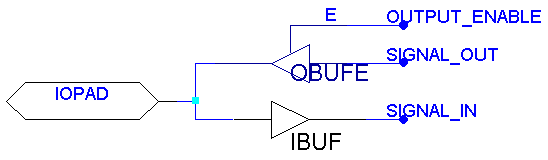
Q: How do you wire bi-directional IO?
A: Use an IOPAD (connnected to a valid bi-directional IO pin, of course), and connect it to an IBUF for the input, and to a OBUFE (tri-state output buffer) for output (a 'T' intersection). Use control logic to enable/disable the output (input is always on, so you input what you output...) using the connection that comes out of the top/side of the triangle (labled E, for enable. 1 = enable, 0 = disable).
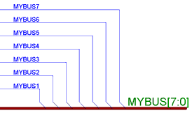
Q: How do you connect single lines to busses?
A: Use a bus tap. To do this, first draw the bus. Then, draw the single
lines, and end them connected to the bus (click on the bus where you want
the connection. You'll see that they connected because the wire gets bent
at the end, to show that it connects to the bus). Now, the bus MUST have
a name. Double click the bus, and give it a name (select a name that has
not been used yet!). Now, select the bus tap tool from the toolbar .
It is right under the bus tool, and looks like a bus with single lines
going off of it to the right (sort of like a comb). Now, click on the bus,
to tell the editor which bus you are tapping. The status bar will now say
"Expand Bus Tap: bus_nameN", where N is the highest numbered line on the
bus. Now, click the single line that you want to be connected to line N.
A label will appear, and the N will decrease by 1. Click on each line until
you are done. Then press escape, or select another tool. Note: N will wrap
around from 0 back to the highest line number, so if you mess something
up, you can just keep clicking until you get the desired number back.
.
It is right under the bus tool, and looks like a bus with single lines
going off of it to the right (sort of like a comb). Now, click on the bus,
to tell the editor which bus you are tapping. The status bar will now say
"Expand Bus Tap: bus_nameN", where N is the highest numbered line on the
bus. Now, click the single line that you want to be connected to line N.
A label will appear, and the N will decrease by 1. Click on each line until
you are done. Then press escape, or select another tool. Note: N will wrap
around from 0 back to the highest line number, so if you mess something
up, you can just keep clicking until you get the desired number back.
[Return to CMPUT 329 Lab Home Page]