CMPUT 329

Lab #1

Simple Alarm System

(2 weeks)


This is an INDIVIDUAL lab. You must complete it by yourself.
Overview:


This lab introduces the Xilinx ISE software, the software we will use for the rest of the term. It also introduces schematic design and VHDL with emphasis on the differences in the design processes therein. In this lab, you design the circuit that controls the alarm system for a home. It is a simple circuit that will help you become familiar with the fundamentals of digital design.

Background:

A house has an alarm system with four sensors: and two state variables:

This alarm system works as follows:
Prelab Assignment:

  1. Reading Assignments:
    1. Read through the lab assignment to familiarize yourself with what you must accomplish.
    2. Read the VHDL FAQ. Also you will want to look at this VHDL tutorial (read the Data Flow Descriptions section for now, don't worry about what a latch is or how it works). Also, be sure to read sections 4.7 - 4.7.2 (p.264 - 271) of the Wakerly textbook.
  2. Logic Equation and Circuit Diagram:
    1. Convert the behavioral description above into a logical equation.
    2. Construct a truth table for this equation. Since the complete truth table would have 26 = 64 lines, you can combine Window and FrontDoor columns into one column that is the OR of the two original columns (W or F), and you can do the same to combine the two motion detector zones (Z1 or Z2).
    3. Draw a sketch of the circuit for this equation.

  1. Schematic Design
    1. Create your project

    2. Create your project and save it in a directory of your choice on the H: Drive. Note: when creating your project, choose the "XST-VHDL" flow type. The settings, as per your board, are:

      XSA-50 Board:
      New Project Window
      You should become familiar with the settings, as you will use them for your board for the duration of the semester.

    3. Create a new schematic
      1. Create a new schematic source

        In the Project menu, select New Source. In the dialog box that opens select Schematic and name your schematic "lab1.sch".

      2. Place the gates

        To place logic gates, select the "Symbols" tab on the left side of the schematic editor and use the scroll box to select the gate that you want to place.Here are some examples and tips to help you out:


        • a 2-input AND gate is called AND2
        • a 3-input OR gate with 2 inverted inputs is OR3B2
        • all inputs and outputs of a gate must be used (ie. don't use a 3-input gate if you only need 2 inputs)
        • to name a net, double click the wire and enter its name
      3. Connect the Gates

        To connect the gates, you need to add wires. Select the wire tool from the toolbar. To draw a wire, move the mouse over the end of the gate pin, and a box should appear. Click on box, and then click on the tip of another pin on another gate. The wire is automatically routed between the two destinations.

      4. Add I/O Pads

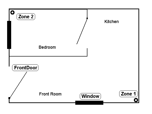
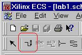
      5. All wires that you want to provide input to or observe output from must be connected to I/O pads. To do this, you must first select the I/O pad tool (selected in the window to the left) from the toolbar. Next, 
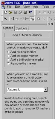
observe the dialog box on the left side.

        These pads determine the inputs and outputs for your design. Moreover, they must be connected to wires on your schematic (they cannot be connected directly to the gate input.)

        Adding in input pad is a simple matter of selecting "Add an input marker" in the dialog on the left side and clicking on the end of the wire whose input you wish to define. From there, you must rename the input pad to correspond to the constraints on your design.

        To rename an I/O pad, you can use one of two methods. The first method is to double click the pad, and then set the net name within the dialog box that appears. The second is to simply right-click on the pad and select Rename from the contextual menu that is brought up. In either case, these names must match with the settings used in the Constraints file, which is detailed later in the lab.

        The additon of an output pad is analogous to that of the input. Select "Add an output marker" and place it on the schematic. Once again, you must rename the pad to match the constraints of your design.


    4. Download the constraints file
      A constraints file describes which pins on the FPGA are to be connected to the signals in your design. Download the constraint file for the XSA-50 board. Save this file as <projname>.ucf:
      Next, Click on Project -> Add sources and add the constraint file to your project. There is another way to define constraints in ISE, and you may refer to the Constraints FAQ for more information.

    5. Connect Input Lines

      The input lines are connected to the parallel port inputs as follows:
      Signal Name GXSPort Button (Used later in lab)
      Window  D0
      FrontDoor  D1
      Zone1 D2
      Zone2 D3
      Home/Away D4
      Armed/Unarmed  D5
      Alarm (output) N/A (middle segment of the LED)

      These connections are made in the constraint file that you have downloaded. To ensure proper connections, make sure that the signal names in your design and in the constraint file are consistent (including the use of upper or lower case). Note: If your signal names are correct, the constraint file should work as is.

    6. Generate the programming (.bit) file and download to the FPGA

      Once you have completed your design, you must create a file that will be used to program the FPGA. To do this, click on the file that you are using (that is, the schematic file) in the hierarchy display on the left side of the ISE window. Next, double click on "Generate Programming File." This will complete the process of creating the .bit file.

      Once the flow manager finishes successfully, you may test your design in hardware. First, we recommend that you test your board using the To download the design to the board, we use the GXSTest utility. Next, open the folder containing your project and drag the '.bit' file into the window of the GXSLoad utility. You must drag your <projname>.bit file from an explorer window to the utility and then click Load.

      To test the design, we will use the GXSPort utility. This utility allows communication with the device through the parallel port. As per the settings in the constraint file, you can use this utility to set the FrontDoor, Window, Zone1, Zone2, Away, and Armed settings. When the alarm is on, the middle segment of the unpaired LED on the board should light up.

      Once you have successfully tested your design, demonstrate to the TA the correctly functioning device. If you are having problems with the implementation, refer to the Common Errors list.


  2. VHDL Design
    1. Create a new VHDL File

      You do not need to create a new VHDL file, but rather simply add a new source to your project using the Project -> New Source menu option. Next, select VHDL Module and name your file 'lab1.vhd'.

      The window that opens allows you to define the inputs and outputs for your design. You can also do this in the editor, but it is simpler for you to enter them here. To create the ports, first click on New and then on the type of port. For incoming signals, such as the Away and Armed signals, the direction is Input. For outgoing signals, such as Alarm, the direction is Output. Do not worry about the other directions or the MSB and LSB, you will deal with these later in the course. Finish entering your seven port names and click Finish Note: Port names must be in ALL CAPS, or there will be conflicts with the constraint file.


    2. Circuit Behaviour

      The wizard has produced an outline of your VHDL code. This outline has to be filled with the behaviour of you circuit. In the area labelled in comments, type in the logical equation description of the Alarm circuit, followed by a semicolon.

    3. Synthesis

      To synthesize your design and ensure that the syntax is correct, simply double-click the Synthesis option in the design flow tree in the bottom-left part of the window.

    4. Further Testing

      For more comprehensive testing, you may use the testbench that we have provided for you. A testbench is a tool that, like a simulator, verifies the logical behaviour of a design. Unlike a simple simulator, however, the testbench allows simple and complete testing of behaviour under all foreseeable conditions. In future labs, we will use this tool extensively to mark your designs. In this lab, however, this portion is purely optional. We do recommend that you do use the testbench to become familiar with its use. To use the testbench, you must create a new project in Sonata and download the testbench files (lab1tb.zip). If you need help with Sonata and using your testbench, consult the Sonata FAQ.

    5. Generate .bit File

      Now, as with part I, you may implement your design by using the Generate Programming File option, and download your design with the GXSLoad utility before testing it in hardware. Once you know that it is working, demonstrate the design so that the TA may sign off on it. Note: Be sure that you have the correct constraint file in the implementation directory.

    6. Questions

      1. Compare and contrast the two methods of designing these circuits (VHDL vs. Schematic design). Which did you prefer and why? What are the advantages and disadvantages of each? How would a larger project affect your choice of method?

    Congratulations! You have completed your first CMPUT 329 Laboratory Exercise.
Report


Complete the questions and, according to the lab report guidelines, complete and submit your report.

Resources

Deliverables

Grading


[Return to CMPUT 329 Lab Home Page]

Created by Paul Berube, 2001, Paras Mehta, 2003.