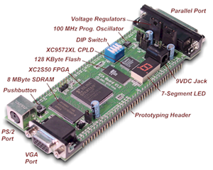
XSA Board From Xess
| Device Family | Spartan2 |
| Device | xc2s50 |
| Package | tq144 |
| Speed | (-) 5 |
| Connection | Pin Assignment | Description |
| Global Clock | p88 | Global clock of the device. It runs at 50 MHz, and is programmable (though you do not need to program it). |
| Reset | p26 | Connected to the reset button on the XStend board. Note: This net is ACTIVE_LOW |
| Spare | p78 | Another button on the XStend board that may be used. Note: This net is ACTIVE_LOW |
| PS/2 Clock | p31 | Clock for the PS/2 port. Note: We provide a component that will handle the keyboard interface for you |
| PS/2 Data | p30 | Port through which the actual PS/2 data enters the FPGA |
| Segment | XStend Left LED (active-low) |
XStend Right LED (active-low) |
Upper LED (active-high) |
Bargraph LED (active-low) |
| 0 | p64 | p47 | p67 | p68 |
| 1 | p65 | p40 | p39 | p44 |
| 2 | p66 | p28 | p62 | p46 |
| 3 | p50 | p29 | p60 | p49 |
| 4 | p51 | p27 | p46 | p57 |
| 5 | p54 | p42 | p57 | p62 |
| 6 | p56 | p48 | p49 | p60 |
| 7 | 67 |
| Address Bit | 0 | 1 | 2 | 3 | 4 | 5 | 6 | 7 | 8 |
| Pin Assignment | p40 | p29 | p28 | p27 | p74 | p75 | p76 | p66 | p50 |
| Address Bit | 9 | 10 | 11 | 12 | 13 | 14 | 15 | 16 | 17 |
| Pin Assignment | p48 | p42 | p47 | p65 | p51 | p54 | p64 | p63 | p56 |
| Data Bit: | 0 | 1 | 2 | 3 | 4 | 5 | 6 | 7 |
| Pin Assignment: | p39 | p44 | p46 | p49 | p57 | p60 | p62 | p67 |
| Signal | Pin Assignment | Description |
| WEB | p58 | Write EnaBle. (active-low) |
| OEB | p43 | Output EnaBle. (active-low) |
| CEB | p41 | Chip select EnaBle. (active-low) |
| RESET | p59 | Flash RAM Reset. (active-low) |
| Port Bit | D0 | D1 | D2 | D3 | D4 | D5 |
| Pin Assignment | p50 | p48 | p42 | p47 | p65 | p51 |
[Return to CMPUT 329 Lab Home Page]