note: always make sure that all the dip switched (blue box with small white sliding switches) are in the "down" (closest to front of board) position, or they can interfere with the proper functioning of your design!
In this lab we will write a small amount of VHDL code to become familiar with the use of VHDL in logic design. We will create a simple XOR parity generator and use it to calculate the parity of hex digits input through the keyboard.
Given a data word formed by n-1 bits, a parity generator is a circuit that generates one extra bit, called the parity bit, to be transmitted along with the data word. The value of the parity bit is determined by the values of the n-1 bits in the data word.
In an even parity scheme, the parity bit is a 1 if there is an odd number of 1's in the data word. Thus when we examine all the bits transmitted (data word + parity), we see an even number of ones, thus "even" parity).
At the receiving end a parity checker is used to detect single bit error in the transmitted data word. The parity checker may regenerate the parity bit in the same fashion as the generator and then compare with the parity bit transmitted. If these two bits do not coincide then at least one of the bits transmitted is incorrect, but the parity checker cannot identify which one. Note that if an even number of bits (2, 4...) are wrong, the single-bit parity scheme will not detect the error.
An even parity generator can be implemented by an n-1 input XOR circuit. The XOR of several bits is one only when there is an odd number of 1's in the source. In our design, we will calculate the parity bit for an 4-bit data word. You are responsible for completing a VHDL module to convert keyboard input into hex values, and creating a VHDL module to calculate the parity of that hex value, and display either a '0' or a '1' on the 7-segment LED on the XS40 board. Also, you will connect the hex value to the bargraph LED on the XStends board for easy confirmation of proper kb -> hex conversion and parity calculation. Keep in mind that the 7-segment LED on the XS40 is active-high, while the bargraph LED on the XStends board is active-low.
You will be provided with a complete VHDL module that implements the keyboard input (KB_INPUT.VHD) and a skeleton VHDL module for the keyboard scanner that converts scanned values to hexadecimal (KB_HEX.VHD). You will simply copy these modules into your project directory and integrate them in your design.
1. There are more than one way to implement an 4-input XOR function using only 2-input XOR gates. Using pencil and paper (ie not the Foundation tools), find the implementation that incurs in the least number of gate delays and the one that incurs in most gate delays between any input and the generation of the output. Sketch the circuits, and compute the number of gate delays to generate the parity bit in each case. Write out the equations as VHDL statements, using brackets to group the gate inputs, beneath the diagrams.
2. Study the schematic diagram presented in this page to understand the whole
design. The goal is to capture key strokes from the keyboard, convert them into
a single hexadecimal digit (4 bits), and display these bits in the bargraph LED
of the XS40 board. In the lab you will be asked to:
a. Create a macro for the
KB_INPUT module (you are given a complete design).
b. Finish the VHDL design of the
KB_HEX module (you are given a partial design), and create a macro.
c. Design, from scratch, the
PARITY module and create a macro.
d. Build the schematic presented in this webpage using the macros that you
created.
e. Simulate, verify,
download to the board, and demonstrate your complete design.
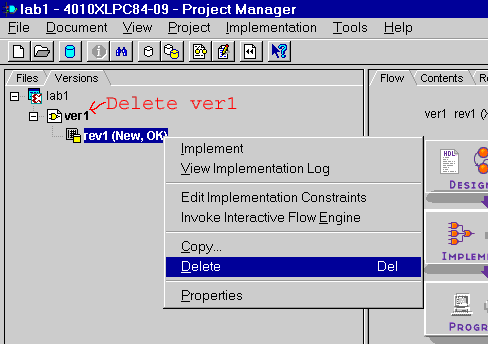
Important: (ignoring this "feature" has caused students
to waste many hours in past years...) The Foundation software that you are using
in this lab tends to not apply your changes to the design, unless you delete
previously implemented versions. Therefore, you must delete
previous versions from the "versions" tab, which appears in the
top left segment of the project manager window before re-implementing your design:
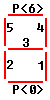
 . Use the wizard to create a VHDL document for a
component named "Parity". The Parity unit should have one input with four
bits: hex[3:0] (hex value from the KB_HEX unit) and one output with eight
bits: P[7:0] (output to the LED). If the number of 1's in the four bits input
is even, then the 7-bit display should show a "0", if there is an odd number
of "1"s in the hex number, than the display should show "1". The
correspondance between the lines of P[7:0] and the segments of the display is
as follows:
. Use the wizard to create a VHDL document for a
component named "Parity". The Parity unit should have one input with four
bits: hex[3:0] (hex value from the KB_HEX unit) and one output with eight
bits: P[7:0] (output to the LED). If the number of 1's in the four bits input
is even, then the 7-bit display should show a "0", if there is an odd number
of "1"s in the hex number, than the display should show "1". The
correspondance between the lines of P[7:0] and the segments of the display is
as follows:
6. Open the HDL editor again, but this time open the KB_INPUT.VHD file. This file contains HDL code to scan the keyboard and detect when keys are pressed. You should read the code to become familiar with HDL code. In order to use this code in your design, you need to create a macro. A macro is an schematic component, which can be inserted into your design the same way as an AND or OR gate. When a macro is created, the HDL source file is synthesized into a gate-level netlist (the code is mapped to a circuit), and a symbol is created from the interface provided in the code. This symbol can later be integrated in a larger design. To create the macro, select "Create Macro" from the Project menu in the HDL editor.
7. Close the editor, and then open it again, this time open the KB_HEX.VHD file. This file is a partially completed module to convert keyboard scancodes into hexadecimal values. Using the PS/2 Keyboard Scancodes provided, complete the definition of the case statement that converts the scancode generated by the KB_INPUT module, named sc in the HDL code, into the hex input for your PARITY module.
Notice that in the first case provided in the file KB_HEX.VHD we converted the key "KP 0", whose code is 70 in hexadecimal (represented as X"70" in VHDL) to the binary number 0000. Remember that you are only specifying outputs for keys that represent hexadecimal numbers, i.e. from "KP 0" to "KP 9" and from "A" to "F" (you may want the keys "0" to "9" to be also interpreted as valid hexadecimal numbers). Once you complete the specification of the case statement in the KB_HEX.VHD file, create a macro for this module. Close the HDL editor.
Your PARITY module will then convert the four bit hex code into the eight
bits P[7:0] signal that will be used to iluminate the 7-segment display.
8. Now go into the schematic editor. You should find all three of your new components at the top of the component library. Use them to create this schematic:
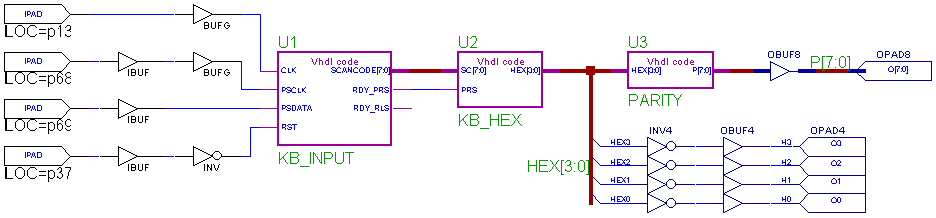
Be sure to use the same names for the output nets, otherwise you will have to edit the ucf file so that the output pins are assigned correctly and you don't get errors when you try to implement the design.
To draw the HEX bus, use the bus tool and click on the bus you already drew between the two modules. Double click to end the bus (at a point where it is long enough). The bus properties window will pop up. Give the bus a name, and make sure it is the right width (ie [3:0]). Then just click on "Bus End". If the name and width do not show up, double click on the bus and enter them again.
9. You have to use inversors to create the signals that will activate the XS40 bargraph (the bargraph is active-low). After inverted these signals are sent to the XStends bargraph through OBUF4 and OPAD4, which are a collection of 4 single components. Because the output of the KB_HEX module is a bus, you need to do a bus tap to connect the four single component inversors to the HEX bus.
10. Save and create the netlist, and implement your design. Then open the Functional simulator and make sure that the parity module behaves properly. You should check the waveform carefully to verify that the behaviour that you expect is being produced before proceeding to download the design to the board. Include the waveform in your report. Important: The KB_INPUT unit is an interface to the PS/2 port. As such, you will not be able to simulate the interaction with this unit (unless you know the PS/2 protocol!). If you want to simulate your entire design (rather than just the individual components), name the SC[7:0] and RDY_PRS lines between the KB_INPUT and KB_HEX units. Then, you can use those lines as your inputs in the simulation.
11. Finally, download your bit file to the FPGA, connect the PS/2 keyboard to the board, and do a hardware test. Once everything works, have the TA sign off on your design.
KB_HEX.VHD Keyboard scancode to hexadecimal value converter. Note: you need to complete this module.
PS/2 Keyboard Scancodes These are the inputs to the KB_HEX module - you need the "make code" values to finish the case statement.
LAB2.UCF
Constraints file for pin assignment on output busses. If you named your project
something other than lab2, rename this file to <projname>.ucf
[Return to CMPUT 329 Lab Home Page]