CMPUT 329

Lab #2

Introduction to Structural VHDL : Parity Checker

(1 week)

This is an INDIVIDUAL lab. You must complete it by yourself.

Updated 26/09/03

NOTE: Make sure that all the dip switches (blue box with small white sliding switches) are in the "down" (closest to front of board) position. Otherwise they may interfere with the proper operation of your design!


Overview

In this lab you will complete the design of a circuit that captures keystrokes from a PS/2 keyboard and converts the keystrokes to hexadecimal values. The binary representation of these values is displayed on the bargraph LED. Another circuit computes the parity of the value and displays it on the right LED of the XStend board

In order to create this functionality, several independent VHDL components must work together. To aid you in creating this design, this lab introduces you to structural VHDL and familiarizes you with several other useful concepts in the VHDL design process.


Background

A parity generator is a circuit that, given an n-1 bit data word, generates an extra (parity) bit that is transmitted with the word. The value of this parity bit is determined by the bits of the data word.

In an even parity scheme, the parity bit is a 1 if there is an odd number of 1's in the data word. Thus when we examine all the bits transmitted (data word + parity), we see an even number of ones (thus "even" parity).

At the receiving end of the transmission, a parity checker uses this extra information to detect single-bit errors in the transmitted data word. It does so by regenerating the parity bit in the same manner as the generator and comparing the two parity bits. Disagreement between these bits means that one of the transmitted bits is incorrect, though the checker cannot determine which bit is in error. Note that single-bit parity scheme is unable to detect an even number of errors (e.g. 4 bits are wrong).

An even parity generator can be implemented by an n-1 input XOR circuit. The XOR of several bits is '1' only when there is an odd number of 1's in the source. Our design calculates the parity of a four-bit word. You are responsible for completing a VHDL module to convert keyboard input into hex values, and creating a VHDL module to calculate the parity of that hex value and display either a '0' or a '1' on the 7-segment LED on the XStend board.

Also, you must display the hex value on the bargraph LED (using the rightmost segments) on the XStends board for easy confirmation of proper kb -> hex conversion and parity calculation. Segments of this LED should correspond to the bits in the hex representation of the value. For example, if the value is 8, only the most significant LED segment should be lit. Keep in mind that the 7-segment LED and the bargraph LED on the XStend board are active-low.

In order to achieve the above functionality, several components must be built. A module to receive and interpret keyboard data is required to translate the PS/2 interface. Moreover, another module must convert the keyboard data to hexadecimal, and a third must calculate the parity of this hexadecimal value for output to the LED. Combining these modules into a single design requires a higher-level VHDL component, which will instantiate the three more basic modules. This higher-level component is written in Structural VHDL. Since this is your first glance at this form of VHDL, you are provided with an outline of the higher-level file which you must complete.

Prelab

  1. Read the lab assignment and become familiar with what's involved. Also, you may wish to read the section in Wakerly on structural design (Section 4.7.6).


  2. There is more than one way to implement a 4-input XOR function using only 2-input XOR gates. Using pencil and paper (i.e. without the Foundation tools), find the implementation that results in the least number of gate delays and the one that incurs the most gate delays between any input and the generation of the output (without redundant or superfluous circuitry, or course). Sketch the circuits, and compute the number of gate delays to generate the parity bit in each case. Write out the equations as VHDL statements, using brackets to group the gate inputs, beneath the diagrams.


  3. Study the written description of the design below and sketch out a block diagram of the connections between the components involved. It is important that you have a good idea about what outputs in one component connect to the inputs of another component before you start working with the design tools.


Lab

Recalling the process from Lab 1, create a new project. Next, be sure to download the files provided and add them to your project. There are four main files, each representing a VHDL module in this project:

KB_INPUT.vhd
Description: We provide this module for you in a completely functional form. It will read the input from the keyboard and produce as output a standard PS/2 representation of the key pressed (note this is not the ASCII code of the character.)
Input:
The global clock (for synchronization), the PS/2 clock and data lines (from the keyboard) and the global reset signals are all inputted to this module. (note: the pushbutton switch labelled reset on the board is active-low. Therefore, when you are using this signal, you must convert it to active-high.)
Output:
The keyboard scancode and a keyboard press signal are the outputs from this module. The scancode contains the information that you need. The keyboard press signal let you know when to read the scancode. Please examine modules that we provide you, to find out that there is a simple and standard way of using this signal

KB_HEX.vhd
Description:
This module is provided as a skeleton only, one which you must complete for yourself. It takes the keyboard scancode as input and converts it to hexadecimal. Invalid digits should produce no change in the module's output.
Input:
The scancode and press signals from the KB_INPUT module are inputted to this module. The press signal facilitates synchronization of the module (i.e. lets the module know when to read the scancode)
Output:
This module outputs the four-bit hexadecimal translation of the scancode.
PARITY.vhd
Description:
You must design this module from scratch. While you may use the VHDL wizard to get a start on this module, the body of the code, which the wizard does not provide, must be written by you. This module calculates parity of the hexadecimal input (which is derived from the keyboard input) and outputs the parity as it would be displayed on the 7-segment LED. Display to the LED is coded by 7 bits as displayed below:

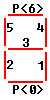
To implement this design, we recommend you use a pair of processes in your code. A process is similar to a function in a traditional programming language; the process runs whenever a signal in its sensitivity list is changed. We recommend that you have one process that calculates the parity bit from the incoming hex signal and another that determines the LED output based on that parity bit.
Input:
The input to this module is the 4 bit hex value.
Output:
A 7-bit std_logic_vector, representing the LED output, is outputted from this module.

Lab2.vhd
Description:
This is a higher level module that describes how the other modules in the design interact with each other. This description is accomplished in Structural VHDL, and involves declaration and instantiation of the modules involved. Moreover, when synthesizing your design, you must ensure that this file is used as the top level design of your circuit.

We have given you most of the information for this design, but you must declare the signals to be used and connect the components correctly.
Input:
All inputs to the circuit must be ports in this file. These are the global clock signal, the global reset, and the PS/2 clock and data signals.
Output:
Similarly to the inputs, all outputs from the circuit must be ports in this file. These outputs are the 7-bit LED signal and the 4-bit hexadecimal signal, which is sent to the bargraph display.


Testing:


As a more thorough test of your design, we have provided a VHDL testbench for this lab, which is used in conjunction with the Sonata software. If you have not used Sonata yet, be sure to read the Sonata FAQ. The waveform produced from this testbench is a required part of your submission (add all signals from the testbench to the waveform and save it.)

Synthesis:

Once all required modules have been created and completed, and they have been added to your project, you may synthesize your project as you did in Lab 1. If you do not recall the settings for synthesis, check the references for the XSA-50 boards.

Implementation:

After successful synthesis of your project, and after ensuring that you have downloaded the correct constraints file and named it correctly in your project folder, you may implement your design.


Deliverables

The following files should be submitted in a zipped file called lab2.zip:

Grading


Resources


[Return to CMPUT 329 Lab Home Page]
Created by Paul Berube, 2001; Modified by Paras Mehta , 2003.