- Runs a test program on the FPGA to make sure everything is working
OK.
Q: When should I run the test?
A: It is probably a good idea to run the test before you start
working, to make sure that everything is set up and working properly.
Also, if you are loading your design into the FPGA, and nothing seems to
be working, try the test. Sometimes, the board stops responding
properly (the Loader still says that the design was loaded
successfully). GXSTest will detect this problem. It can be fixed by
simply unplugging the power jack from the board, and then plugging it
back in. (Re-run the test to be sure).
Q: What does it mean/what should I do if the test fails?
A: Something is wrong with the board setup, or the board itself.
1. make sure that you are testing the correct chip, on the correct
lpt port.
2. unplug the power, then plug it back in (at the board, not the wall
outlet).
3. make sure the parallel cable is firmly plugged into the board and
the computer
4. rerun the test, sometimes it fails for no appapent reason.
5. contact the TA.
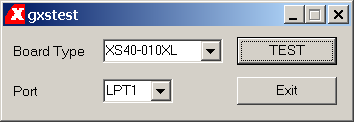
Q: Which Board Type and Port should I use?
A: The Board Type is the XS40-010XL. The Port is LPT1.
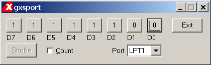
- controls the parallel port so it can be used as input on pins
44-49 of the XS40 board.
Q: The Port utility shows pins D0-D7. How come I can't use D6 and D7?
A: These are mode control pins for the FPGA, and they need to be
connected using special components: MD0 and MD2. In this course, you
won't need to use D6 or D7.
Q: After I load my designs, all the pins are set to 1. But if I have a HEX file with my design, then the pins get set to "random" values?
A: The utility reflects the current state of the parallel port cable
pins. When you load a design, all the pins get set to 1 as the last
step. However, the parallel port is also used to load the HEX file into
RAM, so the final value of the pins in this case is determined by the
last data sent into the RAM. If you are using a HEX file, don't make
your design depend on the initial values of the parallel port pins.
Q: Why is it that I click the buttons, the number changes, but nothing happens in the chip?
A: The numbers on the buttons show you what value the pins will have
AFTER you click the strobe button. Nothing changes until you click
strobe.
Q: What's the count check box for?
A: When this is checked, the port utility acts as a binary counter. Each time you click strobe, the value of the counter goes up by one. Note that you can still change pin values by clicking the buttons, but the counter will increment from that value when you click strobe.
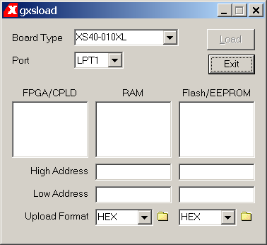
- Loads your design into the FPGA, and can load HEX files into the
external 32K SRAM.
Q: How do I load my design into the FPGA?
A: You MUST drag and drop your .bit file into the loader. As soon as
the file is dropped, the loader will program the FPGA. You can find the
.bit file in your project directory after you successfully implement the
design. It will be called <your_proj_name>.bit . If you have
done this once, however, and you create a new bit file over the old
one, you do not need to reopen the program and reload the .bit
file. You can simply click on load again and your new design into
the board.
Q: How do I load a HEX file into the RAM?
A: The HEX file must be a valid Intel format HEX file. Also, you
must load the RAM at the same time that you load your design. This is
because the design contains information on what chip you are using, and
the HEX file does not. The loader needs to know what chip it is talking
to in order to properly load the RAM. Thus the .bit file is also needed.
You should put the HEX file in the same directory as your project.
Then, select both the .hex and the .bit and drag them (at the same
time) onto the loader. It will then both load the SRAM and program the
FPGA with your design.
Q: What if I want to see the contents of the SRAM?
A: WARNING: this will remove your design from the FPGA!!
You need to use the command line: (in the C:\Xilinx\XSTools directory)
xsload -upload <start_address> <dump_length> <dumpfile.hex> <4010XL.bit>
start_address: first address to grab from
dump_length: number of bytes to dump
dumpfile.hex: the output file (intel HEX format)
4010XL.bit: any bit file for the FPGA being used (for us, the 4010)
you can use your project bit file - it is only needed so
that xsload know what chip it is interfacing with.
eg:
xsload -upload 0 10 dump.hex midi.bit
gets data from address 0 through 9 (10 bytes), puts it in local file
dump.hex (Intel Hex file format).
Q: What is the specification of an Intel Hex file?
A: Try the specs, straight form Intel: Hexadecimal Object File Format Specification (PDF Format)
[Return to CMPUT 329 Lab Home Page]